
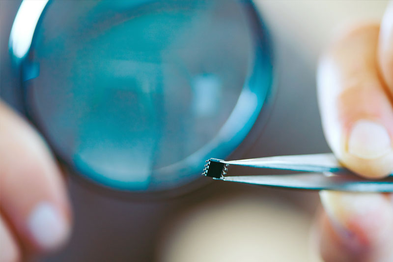
Make the most of smaller components.
Utilize HDIs (high density interconnection) for a higher wiring density per unit area. They’re ideal for using smaller, future-driven components on a wide scale. They offer faster signal transmission and a significant reduction in signal loss and crossing delays – and are ideal for shrinking down the PCB size.
We use a plate-shut process which ensures more reliability for micro via processes as opposed to a process filled with non-conductive ink and then plating over. Our micro via formation technology uses lasers to drill micro vias, also called blind via-holes (BVHs). With the ability to place on or off the pads, these holes let you selectively create routing room in denser parts of the substrate.
The benefits of HDIs.
- Increase electrical performance: The smaller parts used on HDI boards have shorter internal wire lengths. This provides reduced rise times and lower power requirements when compared to their larger, alternative packages.
- Reduce PCB size. HDIs create a gateway to miniaturization of PCB design with ‘via in pad’ technology.
- Improve reliability by stepping up technology rather than compromising existing design rules.
- Gain design choices when it comes to BGA layout with the smallest pitch.
- Increase thermal enhancement.
- Increase interconnection density by reducing plated thru holes, pad size and conductor size.